


The chip design process has historically been a labour-intensive and skill-heavy sector. For decades, the creation of semiconductor devices required teams of highly skilled engineers working meticulously through every stage of development—from initial design conceptualization to final manufacturing.
The intricacies involved in crafting circuits, designing architectures and ensuring flawless execution demanded a depth of expertise that few possessed. Engineers spent countless hours manually iterating and optimizing designs to meet stringent Performance, Power and Area (PPA) requirements.
This laborious process has always been limited by the availability of skilled manpower and the inherent complexities of the task. Additionally, the turn-around-time (TAT) for the entire Design to Fab process takes months to be able to come up with a viable chip specialized for a specific purpose.
However, the semiconductor landscape is undergoing a significant transformation – driven by the explosive growth of compute-intensive applications such as artificial intelligence, high-performance computing and autonomous vehicles.
These advancements demand increasingly complex chips capable of delivering unprecedented levels of performance and efficiency. The rise of devices featuring billions of transistors and angstrom-scale structures has added new layers of complexity to chip design. Simultaneously, the industry faces a critical shortage of engineering talent, threatening to stall the innovation that fuels technological progress.
Generative AI and Large Language Models are ushering in a new era of efficiency and innovation in chip design. By automating routine tasks, providing contextual guidance, and enhancing data-driven decision-making; these technologies can empower engineers to tackle the complexities of modern semiconductor design in a more autonomous and efficient way, so that the designing focus can go back to where it matters most – Differentiation!
Specifically, GenAI can make a significant impact on the following areas in the design lifecycle:
Design Space Exploration
GenAI can rapidly explore vast design spaces to identify optimal configurations. By analysing a wide range of parameters, it can suggest design variations that meet specific criteria for PPA; thus significantly accelerating the design process.
RTL Generation and Optimization
Register-Transfer Level (RTL) design is a critical phase in chip development. GenAI can generate RTL code from high-level specifications, reducing manual coding efforts and minimizing human errors. Additionally, it can optimize existing RTL designs to improve efficiency and reduce resource consumption.
Verification and Testing
Verification is a time-consuming process that involves checking the correctness of a design over multiple iterations across multiple parameters. GenAI can automate the generation of test cases, improve verification coverage and autonomously analyse results to identify potential issues and take corrective action. This automation reduces the time and effort required for the entire V&V lifecycle.
Analog Design Automation
Traditionally, analog design has been a highly manual and iterative process requiring highly specialized skills. GenAI can automate many aspects of analog design; such as optimizing circuit parameters and migrating designs across technology nodes, thus improving productivity and reducing time-to-market.
LLMs on the other hand have a very unique value proposition for the chip design industry. It has the potential to help bridge the skill gap within the existing RTL design workforce. Not just that, it is capable of extracting and deploying differentiated knowledge specific to a chip manufacturer’s IP while in the design process to accelerate design viability.
Following are few value propositions that LLMs bring to the chip design community:
Knowledge Query Systems
LLMs can act as interactive knowledge base; offering answers to engineers’ questions about design methodologies, tool usage and troubleshooting withing the manufacturer’s IP limitations. This capability reduces the need to sift through extensive documentation or knowledge exchange, thus streamlining the problem-solving process.
Contextual Assistance
By understanding the context and limitations of a specific design challenge, LLMs can offer tailored guidance and suggestions. For example, if an engineer is working on optimizing a particular aspect of a chip, the LLM can provide relevant tips and strategies based on past successful designs.
Workflow Automation
LLMs can assist in automating repetitive tasks by generating scripts and workflows that enhance productivity. This automation extends to creating design verification scripts, setting up simulation environments and configuring design tools in an autonomous fashion.
Natural Language Specifications
LLMs can translate natural language specifications into design elements, enabling engineers to describe their design goals in everyday language and receive detailed design suggestions or implementations. This capability bridges the gap between conceptual ideas and technical execution.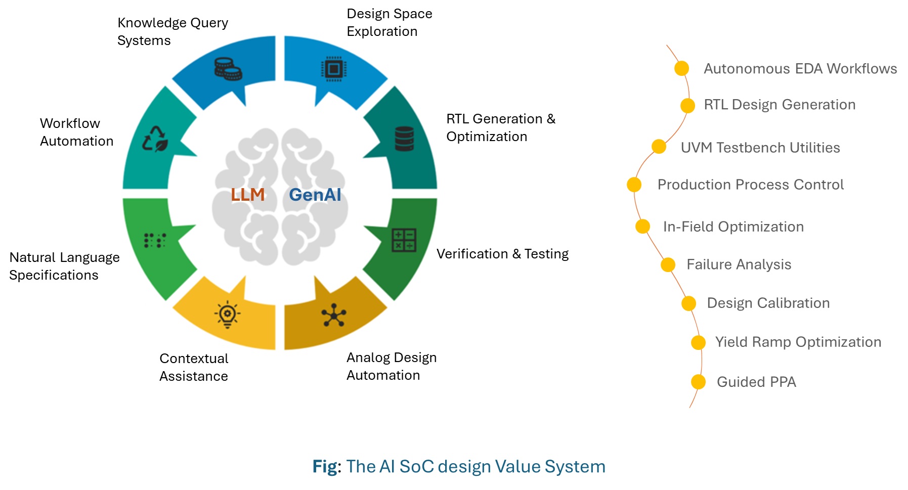
The Future:
AI systems will become increasingly autonomous and capable of managing entire design cycles from architecture to manufacturing, noted Saurabh, SmartSoC. This autonomy will reduce the need for manual intervention and increase design efficiency. Engineers will be able to describe design goals and requirements using natural language, with AI systems translating these descriptions into detailed design implementations.
This capability will democratize chip design, making it more accessible to a wider range of innovators. By facilitate collaboration between design teams by providing real-time insights and recommendations; it will foster innovation and accelerate the development of cutting-edge semiconductor technologies. The integration of GenAI and LLMs will not only address the challenges posed by the engineering talent shortage but also pave the way for unprecedented levels of productivity and innovation in the semiconductor industry.
About The Author:
Saurabh Chakraborty, VP & Head of Artificial Intelligence at SmartSoC. He has 20 years of experience in AI, Digital and EdgeAI domains.