


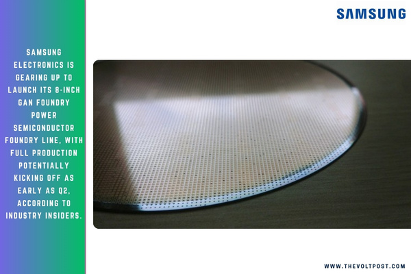
Samsung Electronics is gearing up to launch its 8-Inch GaN Foundry power semiconductor foundry line, with full production potentially kicking off as early as Q2, according to industry insiders.
This step comes over three years after Samsung first announced its GaN ambitions, and they’ve already lined up their first customer though revenue is expected to stay modest, under 100 billion won, given the narrow client base so far.
Samsung’s approach is a turnkey service that skips chip design to boost margins. They’re making their own wafers in-house too, having nailed down mass-production-ready epitaxial (epi) wafers after initially sourcing them externally during pilots. GaN wafers blend gallium and nitrogen for specialized power needs.
Meanwhile, rival DB HiTek offers similar wafer-plus-foundry combos but outsources packaging, with mass production slated for the second half of the year trailing Samsung by a quarter or two. SK Keyfoundry is eyeing the space too, but not ramping up anytime soon.
Power semis split mainly into GaN and silicon carbide (SiC) materials. Both beat traditional silicon with wider bandgaps for superior voltage handling and efficiency.
 GaN shines in sub-1,200V apps like EV chargers, phone adapters, and AI data center power conversion think Nvidia’s push for 800V DC architectures, where GaN converters step down voltage efficiently with fast switching, higher density, less heat, and smaller footprints.