


Renesas Electronics Corporation has unveiled a new configurable 3nm TCAM.
Built on an advanced 3nm FinFET process, it achieves a rare combination of high density, low power consumption, and enhanced functional safety. The 3nm ternary content-addressable memory (TCAM) breakthrough, presented at the 2026 International Solid-State Circuits Conference (ISSCC) in San Francisco, positions the technology for both networking and automotive system-on-chip (SoC) applications.
As data traffic continues to surge with the growth of 5G and cloud-edge computing, large-scale TCAMs have become essential for high-speed data lookup and packet classification.
Traditional approaches that scale TCAM capacity by simply adding banks or repeaters tend to increase peripheral area and search power, while making timing closure more difficult.
Automotive applications add another layer of complexity, demanding stringent functional safety standards like ISO 26262. Renesas’ 3nm TCAM tackles all these challenges head-on with several key innovations.
Flexible, High-Density TCAM Architecture
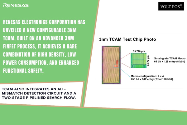
Renesas combines hard-macro design with software-configurable generation tools, offering TCAM configurations at a fine granularity from 8- to 64-bit key widths and 32- to 128-entry depths.
Larger instances, such as 256-bit × 4,096 entries, can be seamlessly built by combining these building blocks through automated soft-macro generation.
This hybrid “hard and soft” approach enables a flexible single macro that adapts to a wide range of system requirements while maintaining an industry-leading memory density of 5.27 Mb/mm².
Smarter Search Processing for Low Power
The TCAM also integrates an all-mismatch detection circuit and a two-stage pipelined search flow. Depending on the first-stage result, the system can halt the second stage early, reducing unnecessary energy consumption.
In typical configurations, 64–256-bit widths and 512-entry depths, this technique slashes search energy by up to 71.1% (with column-wise pipelining for keys above 64 bits) and up to 65.3% (with row-wise pipelining for smaller keys).
Operating at a 1.7 GHz search clock, the design achieves just 0.167 fJ/bit of search energy in a 256-bit × 512-entry setup. This delivers a remarkable TCAM figure-of-merit of 53.8 (density × speed ÷ energy), surpassing previous designs.
Strengthened Functional Safety for Automotive Systems
Because TCAM cells for the same address sit physically close together, they are vulnerable to double-bit errors from radiation-induced soft faults, errors that conventional SECDED ECC cannot correct. Renesas mitigates this with two clever techniques:
-
Split data buses: Odd and even data lines are separated for user data and ECC parity, spreading the physical layout to convert double-bit faults into correctable single-bit ones.
-
Dedicated ECC SRAM: A separate SRAM stores ECC parity bits, running its own address decoding process, which helps detect incorrect address selections during write operations.
 These design choices dramatically improve safety coverage, making the TCAM robust enough for the reliability standards demanded in automotive environments.
With its combination of configurable precision, low power, and high dependability, Renesas’ new TCAM design isn’t just aimed at next-gen driver-assistance or autonomous systems, it’s equally suitable for industrial and consumer devices that rely on fast, reliable data processing.
The company plans to continue developing scalable memory architectures that push the boundaries of performance, efficiency, and safety.
To Know More: CLICK HERE