Rapidus Corporation declared that it will establish a clean room at the Chitose, Hokkaido, headquarters of Seiko Epson Corporation and launch Rapidus Chiplet Solutions (RCS), an R&D center for semiconductor post-processing.
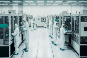
The Rapidus Innovative Integration for production (IIM) foundry, which Rapidus is presently constructing in Bibi, Chitose City, is located next to the Seiko Epson Chitose Plant.
This is the semiconductor production facility. Recent groundbreaking ceremony revealed the new R&D space, which includes a clean room spanning roughly 9,000m2 (96,875 square feet). Using the new R&D center, Rapidus will create chiplet packages for mass production technologies.
April 2025 will see Rapidus start installing production equipment, while April 2026 will see the start of R&D. Pilot lines for the FCBGA, Si interposer, RDL, and hybrid bonding processes will be available at RCS.
Apart from post semiconductor processing, the company will also carry out further research and development on mass production technologies, such as equipment automation.
The project for the “Development of Chiplet Package Design and Manufacturing Technology for 2nm Generation Semiconductors” was approved in April 2024 by the Ministry of Economy, Trade and Industry, New Energy, and Industrial Technology Development Organization. Development of core technologies, including chiplet integration and 2.5D/3D packaging, is also moving forward.
The Japanese Semiconductor Manufacturer and IBM partnered in June 2024 for chiplet technology as well as front-end procedures.