


RECOM has released a product named the RxxC2T25S. It is an SMD DC/DC converter in a SOIC package with an integrated isolation transformer. To allow the designer to switch easily between first and second-source power transistor suppliers by changing the BoM resistor values, but not the PCB design.
There is an increasing demand for improved efficiency at higher output power levels for automotive, industrial and inverter applications.
For electric vehicles (EVs), this improvement is essential for extending the performance and range through more efficient motor drives and faster battery chargers.
For industry, improved efficiency is crucial for the reduction of the global energy consumption and to improve sustainability, hence the current focus on the efficiency benefits of DC microgrid technology.
For green renewable energy, high efficiencies foster the uptake of photovoltaic, water, and wind generation, extracting the maximum energy from limited natural resources.
To achieve this essential efficiency objective, power electronics is transitioning to higher switching frequencies and increased voltages, while still trying to balance the cost vs performance equation and to reduce the overall size (Figure 1).
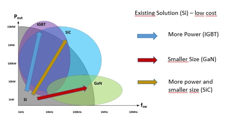
However, such a transition necessitates the integration of next-generation semiconductor devices, with new iterations of power MOSFETs and wide-band gap SiCs and GaNs being released on a regular basis.
This poses a challenge for design engineers:
In an environment marked by constant advancements in power switching transistor technology, how can I future-proof my power stages to take advantage of these new generations without the need for constant redesign?
Let us take a typical power design requirement as an example:
A solution is needed for an advanced three-phase battery charger for EVs with high efficiency and small size.
The Power stage should be bi-directional and should be equally efficient in both directions from AC-to-DC and from DC-to-AC. The AC side should feature active power factor control (PFC) and the DC side should have low switching losses and interface with battery packs with voltages up to 800VDC. The design should operate at a high switching frequency to reduce the size and weight of the inductive components.
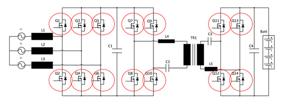
A possible solution incorporating a three-phase PFC, full-bridge bidirectional LLC and active rectifier is shown in Figure 2. This solution requires fourteen power transistors, which for optimal cost vs performance could be a mix of MOSFET, SiC, and possibly GaN devices.
All the power transistors will need individual gate drivers, with the high side transistors (Q1, Q3, Q5, Q7, Q9, Q11 and Q13) also needing galvanic isolation. If the gate drivers have separate Out+ and Out- pins, then different gate resistors for the on and off cycles can be used to optimise the switching characteristics.
Also, the isolated Vpos and Vneg voltages can be chosen to fully enhance the transistor during the on-cycle and rapidly discharge the gate capacitance during the off cycle. A negative “off” voltage also makes the switching more reliable by eliminating false turn-on due to source inductances1.
Therein lies the problem: different switching technologies and transistor generations have different recommended and absolute maximum gate drive levels (Figure 3).
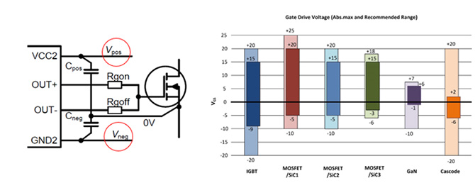
A gate driver design that was optimized for IGBTs with asymmetric supply voltages of +15/-9V would severely stress a first or second generation SiC with only 1V headroom to the negative abs. max. limit and not work at all with a third generation SiC transistor.
A similar problem exists with a design that needs to transition from a first-generation SiC to a second or third-generation SiC – the +20V positive rail would be the same as or exceed the abs. max. limit of the newer generations, leading to early failure.
The tendency is that each new generation of power transistor will be fully enhanced or fully depleted with lower gate drive voltage levels, but the optimal gate drive voltage levels will still vary between manufacturer, development iteration and transistor type.
As the isolated gate driver power supply voltage (Vpos and Vneg) is provided by either an isolating transformer or an isolated DC/DC converter, different solutions will be required for each power transistor selection, even though the gate driver itself is useable for all transistor types.
This means that even using a pin compatible second source switching transistor may require significant design changes in the isolated power supply.
What is needed is a programmable isolated asymmetric power supply to allow the gate driver circuit to be optimised for different transistor options, possibly including new generations that have not even been released yet.
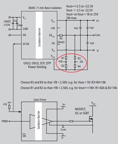
RECOM has released such a product: the RxxC2T25S. It is an SMD DC/DC converter in a SOIC package with an integrated isolation transformer (Figure 4).
The outputs of SMD DC/DC converter can be independently set in the range between +2.5V to +22.5V and from -2.5V to -22.5V by changing resistor values in a feedback divider circuit, meaning that one power supply solution can provide +15/-9, +20/-5, +18/-4, +15/-3 or any other output voltage combination as long as the combined output lies in the range of 18 to 25V.
This allows the designer to switch easily between first and second-source power transistor suppliers by changing the BoM resistor values, but not the PCB design. It also means that if a completely new generation of power transistor is released with, say, +14.5/-3.5V optimal gate drive voltages, the solution is future-proofed.
Finally, the output voltages are independently regulated, essential when driving the gate to voltages which are very close to the abs. max. levels to get the highest possible switching efficiency.

As power levels increase into the kilowatt levels, the environment around the gate driver and gate driver power supply becomes harsher. Despite the low switching losses of advanced WBG power transistor technologies, high ambient operating temperatures are to be expected.
Hard switching of high voltages creates very high dv/dt slew rates, so good CMTI (Common Mode Transient Immunity), low isolation capacitance and high isolation is essential for robust switching reliability.
The RxxC2T25S SMD DC/DC converter features an ambient operating temperature range of -40°C to +100°C with 1.5W load, and up to +125°C with 0.6W load, an impressive CMTI of ±150kV/µs. The Recom SMD DC/DC converter delivers an isolation capacitance of only 3.5pF and 3kVAC/1minute isolation (also rated for ±1200VDC repetitive peak voltage). The outputs of SMD DC/DC converter are also fully protected against short circuit, overload, and over-temperature.
An under-voltage lockout function means that the DC-OK pin only becomes active once both the input voltage and output voltages have been stabilised, so this pin can be connected to the enable pin on the gate driver to ensure that conditions are stable from the very first switching cycle (figure 5).
In conclusion, the RxxC2T25S SMD DC/DC converter is a solution that designers have been waiting for. A robust SMD part that is specifically designed for isolated gate driver applications with all the technical features one might expect and the benefit of being able to freely choose the output voltages to get the maximum efficiency out of existing solutions as well as future designs.
ARTICLE SOURCE: RECOM POWER
