


Using its in-house CFB technology, OKI has effectively developed Tiling Crystal Film Bonding (CFB) technology. This method will help progress the quickly expanding field of photonics-electronics convergence technology by enabling the heterogeneous integration of small-diameter optical semiconductor wafers onto 300 mm silicon wafers, which was previously impossible due to wafer size limits.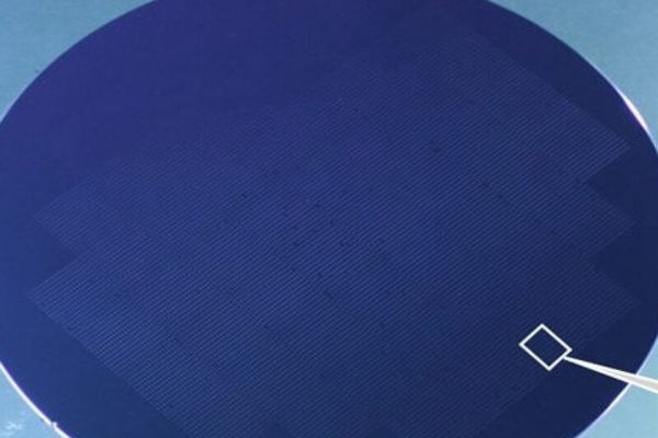
OKI wants to work with universities and partner companies to achieve early commercialization.
Suppressing increases in power consumption while increasing data processing capabilities is a major social concern because of the recent rapid advancements in artificial intelligence (AI), which have increased demand for data centers. Technologies that offer high density, high speed transmission, and low power consumption by utilizing photonics-electronics convergence technology—which blends electrical and optical circuits—are one way to address this issue.
Specifically, it is anticipated that the integration of silicon photonics (Note 3) with optical semiconductors will be made possible by the heterogeneous integration of optical semiconductors onto silicon wafers, which will further enhance performance.
However, there are a number of technical difficulties with heterogeneous integration.
For instance, optical semiconductor wafers like InP (indium phosphide) wafers are usually smaller 50 mm (2-inch) to 100 mm (4-inch) compound semiconductor wafers because of the challenge of achieving epitaxial growth, whereas silicon photonics uses large-diameter silicon wafers of 200 mm (8-inch) or 300 mm (12-inch). Furthermore, nanoscale roughness control is necessary for silicon optical waveguides, necessitating damage-avoidance heterogeneous integration procedures.
This difference in wafer sizes is resolved by OKI’s Tiling CFB technology, which permits heterogeneous integration without resulting in damage. The approach makes efficient use of InP-based materials by enabling 52 repeated tiling processes over the whole surface of a 300 mm silicon wafer using a single 2-inch InP wafer.
After transfer, the InP wafer can be used exactly as is, allowing for material recycling and reuse and lessening the impact on the environment. With an angular accuracy of ±0.005°, the placement accuracy is roughly ±1 ?m.
High-efficiency optical coupling between optical semiconductors and silicon waveguides is made possible by this high accuracy in conjunction with OKI’s exclusive 3D intersecting waveguide silicon photonics technology.
In a demonstration, InP-based Crystal Films and a sacrificial layer that served as optical semiconductors were produced epitaxially on a 2-inch InP wafer and subsequently divided into discrete elements.
On each element, a support structure for batch transfer and a protection structure to guard against chemical assault during etching the sacrificial layer were created. This made it possible to successfully and erosion-free batch transfer the InP-based Crystal Films to an intermediate transfer substrate.
Since removing the support and protective structures from the intermediate transfer substrate shields the silicon wafer from harm during the removal process, batch transfer to an intermediate transfer substrate is done to protect the silicon wafer from harm during the subsequent removal process.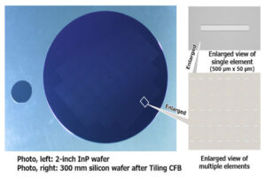
The InP-based Crystal Films are guaranteed to remain adherent while the protective and support structures are being removed, not peel off, and transfer effortlessly thanks to the special design of the intermediate transfer substrate.
Additionally, OKI developed Tiling CFB technology, which allows tiling over a 300 mm silicon wafer’s whole surface, by repeatedly transferring Crystal Films from the intermediate transfer substrate using a CFB stamp. Only the necessary Crystal Films may be transferred selectively by the CFB stamp’s structure, and efficient tiling is made possible by repeated transfers.
Effective material utilization without waste is made possible by the ability to repeatedly transfer lower-density arrays of Crystal Films needed for the device from a high-density array of Crystal Films formed on the intermediate transfer substrate.
The CFB stamp used in this demonstration, which was 30 mm by 30 mm, finished 52 transfers into a 300 mm silicon wafer’s whole surface in around 10 minutes, which is plenty for commercial manufacturing.
Tiling CFB technology’s viability in transferring from 2-inch to 300 mm silicon wafers was demonstrated by this demonstration. Additionally, the technique may be modified as needed to work with 200 mm silicon wafers and 3- or 4-inch InP wafers.
It will assist increase productivity by enabling the use of larger wafer sizes and performance by enabling transfer to high heat-dissipation substrates because it can also be used with current optical semiconductor devices.
Additionally, tiling CFB technology will lessen the environmental impact and enhance photonics-electronics convergence technology. In order to achieve early commercialization of the technology, OKI intends to improve cooperation with device manufacturers.