


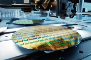
Wafer or semiconductor fabrication is the intricate process of creating semiconductor devices. As per the rising need and demand for complex and advanced semiconductors, the complexities of wafer fabrication also increase.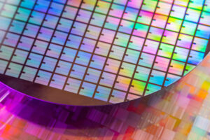
Wafers are used across various industries like automotive, consumer electronics, aerospace & defense, healthcare, and telecommunication. According to the Consegic Business Intelligence analysis, Wafer Fabrication Market size is estimated to reach over USD 105.98 Billion by 2031 from a value of USD 67.81 Billion in 2022 and is projected to grow by USD 69.86 Billion in 2023, growing at a CAGR of 5.3% from 2023 to 2031.
Challenges
-
Miniaturization and Scaling
As technology nodes shrink to below 10 nanometers, it becomes increasingly challenging to control critical dimensions and minimize defects. Quantum effects such as electron tunneling and variations in electrical characteristics can cause unpredictable transistor behavior, impacting chip reliability and performance.
As features on the wafer become smaller, the resolution of photolithography systems must increase, pushing the limits of optical physics. This makes it harder to maintain pattern fidelity, leading to variations that can affect circuit performance.
-
Material Limitations
Traditionally, materials like silicon are used for wafer fabrication but they are reaching their physical and performance limits, especially in power and high-frequency applications.
New materials like silicon carbide (SiC), and gallium nitride (GaN) are being explored as they offer superior electrical properties. SiC operates at higher voltages and temperatures, making it ideal for power electronics in electric vehicles and renewable energy sources.
However, these materials introduce new challenges for wafer fabricaton. SiC is harder but more brittle than silicon, complicating the wafer slicing and polishing. Moreover, GaN needs an additional buffer layer when grown on silicon wafers, further increasing the complexity of the manufacturing process.
-
Complexity and Cost
Advanced processes, such as extreme ultraviolet (EUV) lithography, are essential for cutting-edge nodes. These processes involve sophisticated, expensive equipment that requires high levels of expertise to operate.
The development and maintenance of such equipment add to the overall cost of the process. Additionally, building more fabs continues to rise in cost, with state-of-the-art facilities now costing upwards of $20 billion.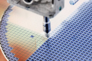
This high investment makes it difficult for smaller companies to compete, leading to increased consolidation in the industry.
-
Defect Density
With increasing wafer sizes (for example from 300nm to 450 nm), maintaining low defect densities is crucial. Lager wafers are more prone to contamination and defects, impacting yield and profitability.
Each defect on a larger wafer can affect more chips, making stringent contamination control essential. Effective defect detection and correction systems are challenging to implement.
They require sophisticated equipment and methodologies to identify microscopic defects and address them without impacting the overall manufacturing process is key for wafer fabrication.
-
Environmental Impacts
The semiconductor industry consumes significant amounts of water and energy to operate. A single fabrication unit uses millions of gallons of ultrapure water every day. This also produces a significant amount of wastewater.
Additionally, the chemical processes involved in the fabrication produce hazardous waste that must be carefully managed. Reducing the environmental footprint while maintaining production efficiency is a growing concern.
This involves reducing resource consumption and improving waste management and recycling processes.
Solutions
-
Advanced Lithography
Extreme ultraviolet (EUV) lithography has become crucial for scaling down to 7nm and beyond. Ongoing improvements in EUV technology, such as higher power sources and better photoresists, are essential for future nodes.
Advances in mask design and pellicles are helping to reduce defects and increase yield. Additionally, the use of multi-patterning techniques, which involve multiple lithography steps to define small features, is enabling us to surpass the limits of traditional lithography.
Though this approach requires precise alignment and control, it allows for the continued scaling of device features.
-
New Materials and Processes
Research into alternative materials such as SiC and GaN offers the potential for increased performance and efficiency, especially in the field of power electronics. Shifting from silicon to these materials involves the development of new wafer fabrication techniques and equipment.
For instance, high-temperature processes are necessary for SiC, while GaN requires specific epitaxial growth methods. The integration of these new materials with existing silicon technology is also a priority.
Hybrid devices that combine the best properties of different materials are being developed to enhance performance for specific applications.
-
Process Control and Metrology
Advanced metrology and inspection tools are crucial for early identification and mitigation of defects in the manufacturing process.
Techniques such as in-line monitoring and machine learning for predictive maintenance are enhancing yield and reducing downtime. Real-time data analysis facilitates immediate adjustments, thus minimizing the impact of variations.
Atomic-level metrology, utilizing tools such as scanning electron microscopes (SEMs) and atomic force microscopes (AFMs), offers detailed insights into surface topography and material composition, ensuring that each wafer layer meets strict specifications.
-
3D Integration
3D integration and packaging, such as through-silicon vias (TSVs) and chiplet architectures, provide solutions for performance and scaling challenges.
These approaches allow for higher density and improved electrical performance without the need for further shrinking the individual components. Advanced packaging techniques, such as wafer-level packaging and system-in-package (SiP), are being developed to integrate multiple chips into a single package.
This reduces interconnect length and improves signal integrity, ultimately enhancing overall system performance.
-
Sustainable Practices
Fabs are implementing efforts to reduce water and energy consumption. This includes recycling and reclaiming water, using renewable energy sources, and optimizing processes to lower emissions.
Green fabs are designed to minimize environmental impact through energy-efficient lighting, heating, and cooling systems. The industry is also exploring the use of alternative, less hazardous chemicals in the fabrication process.
Developing more sustainable manufacturing processes can help reduce the environmental footprint while maintaining high levels of production efficiency.
Conclusion
The field of wafer fabrication is constantly advancing due to the increasing demand for smaller, faster, and more efficient semiconductor devices. While there are challenges such as scaling limitations and material constraints, the wafer fabrication industry is responding with innovative solutions and collaborative efforts.
Progress in lithography, new materials, AI-driven automation, and sustainable practices are shaping the next generation of semiconductor technologies. As research continues and new technologies emerge, the future of wafer fabrication appears both challenging and promising.
Author Bio: I’m Jayesh, a Professional Content Writer at Consegic Business Intelligence, with expertise in Semiconductor and Electronics Industry.
Source: Consegic Business Intelligence – Wafer Fabrication Market