


The Xilinx Artix-7 XC7A100T FPGA chip powers the latest embedded System-On-Module (SoM) from MYIR, the MYC-J7A100T, which has a fast and high-density circuit board design.
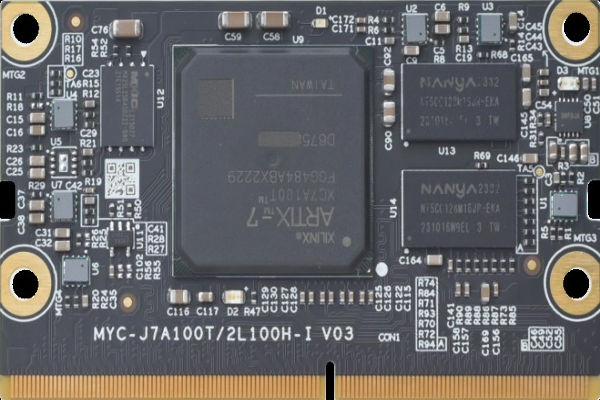
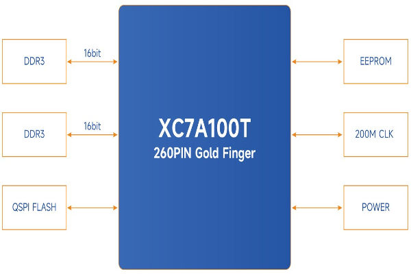
The small 69.6mm × 40mm SOM module is packed with integrated circuits, including DC-DC power management, 512MB DDR3 memory, 32MB QSPI FLASH, 32KB EEPROM, and other essential circuits. It is powered by the XC7A100T-2FGG484I chip.
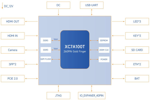
Numerous connecting possibilities are available via its 260-pin extension interface, which uses an MXM Gold-finger-edge-card interface. In order to provide easy integration and flexibility, this interface offers four pairs of GTP high-speed transceiver interfaces, 178 FPGA IOs, and a JTAG interface.
Out of the 178 FPGA IOs, 80 run at 3.3V, while the other 98 may be user-configured to run at different voltage levels (1.2/1.35/1.5/1.8/2.5/3.3V) to accommodate different application needs. MYIR It may be used in many different sectors, including as computer, automation, communication, and industrial control.
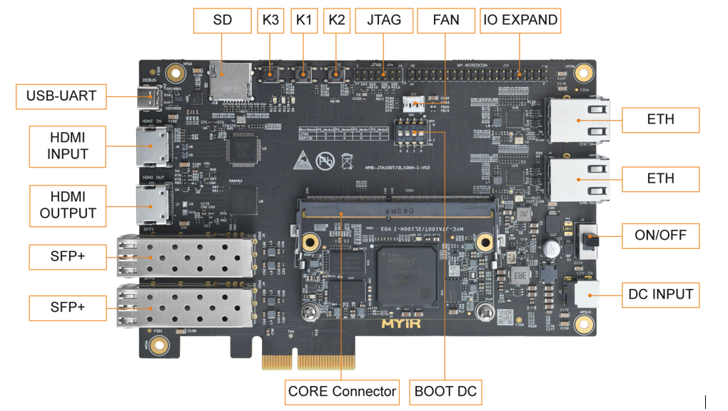
The MYD-J7A100T development board, available from MYIR, is a great tool for testing the MYC-J7A100 SOM. A wide variety of communication interfaces are available on the board, which is centered around the MYC-J7A100T.
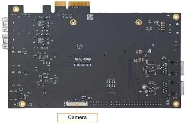
These interfaces include a USB-UART, two Gigabit Ethernet ports, two SFP+ interfaces, a PCIe 2.0 slot, a Micro SD card slot, an HDMI input and output, a DVP camera interface, and an IO expansion interface.
A USB Type-A to Type-C connector, a 12V/2A power adapter, and a Quick Start Guide are included with the MYD-J7A100T development board.
To improve functionality, MYIR provides optional add-ons like the MY-CAM011B Camera Module and the MY-WIREDCOM RPI Module. MYIR helps customers to rapidly begin working on their solutions by offering a variety of Vivado example codes for testing. It is a solid and trustworthy reference design for Xilinx Artix-7 XC7A100T solutions development.
Powered By Xilinx Artix-7 XC7A100T FPGA Chip, the MYC-J7A100T SOM Features:
- Dimensions: 69.6mm (L)× 40mm (W)
- PCB Layers: 12-layer design
- Power supply: 5V / 3A
- Working temperature: -40~85 Celsius (industrial grade)
- Xilinx Artix-7 XC7A100T FPGA (XC7A100T-2FGG484I)
– Logic Cells 101,440
– Block RAM 4,860kb
– DSP Slices 240
– 8 GTP transceivers capable of reaching speeds up to 6.6Gb/s
– x4 Gen2 PCIe interface - 512MB DDR3
- 32MB QSPI FLASH
- 32KB EEPROM
- DC-DC power management
- 260-pin MXM gold-finger-edge-card expansion interface
Availability and Pricing
For the MYC-J7A100T, MYIR provides the standard part MYC-J7A100T-32Q512D-I. At an affordable $125, this component boasts 32MB of QSPI storage and 512MB of DDR3 RAM. Moreover, bulk discounts are offered for more affordable shopping choices.
For Further Info About the MYC-J7A100T SOM: CLICK HERE
