


The new materials engineering advances from Applied Materials are intended to boost computer systems’ performance-per-watt by allowing copper wiring to scale up to the 2nm logic node and beyond.
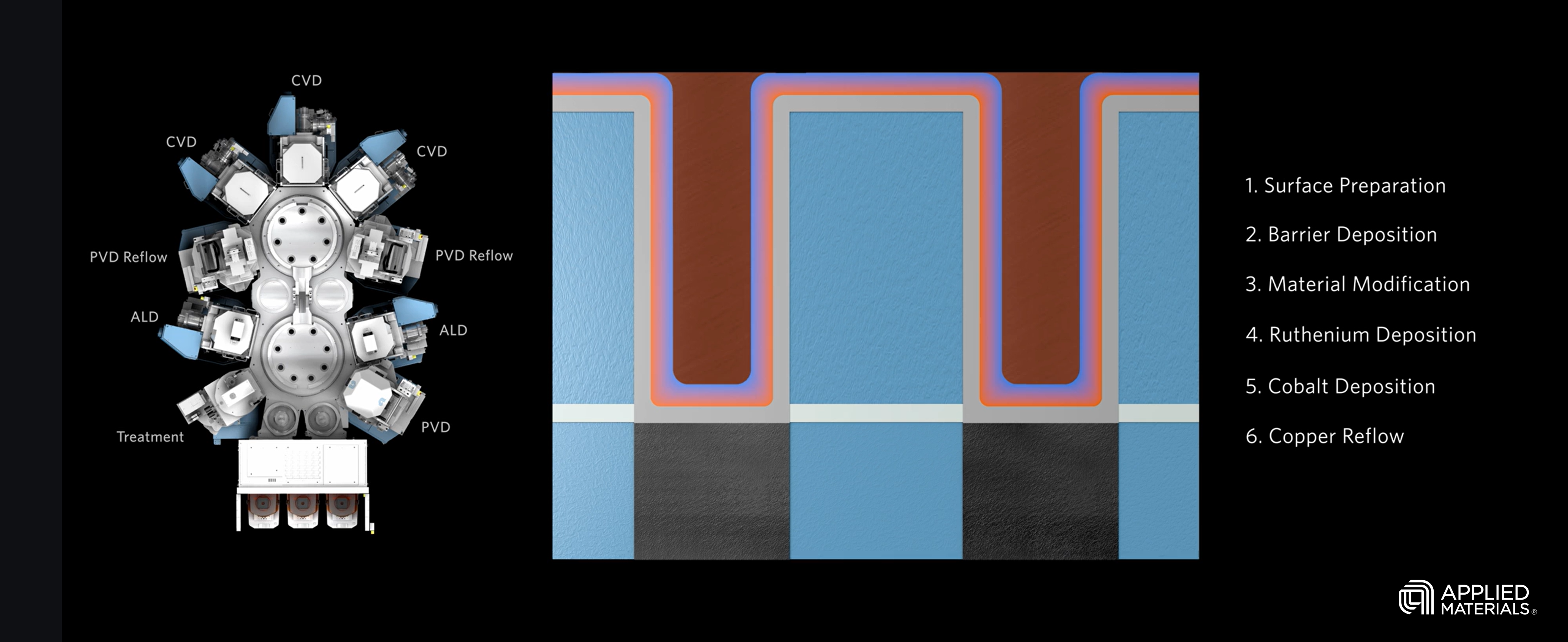
Applied Materials’ new Endura™ Copper Barrier Seed IMS™ with Volta™ Ruthenium CVD combines six different technologies in one high-vacuum system, including an industry-first combination of materials that enables chipmakers to scale copper wiring to the 2nm node and beyond.
“The AI era needs more energy-efficient computing, and chip wiring and stacking are critical to performance and power consumption,” said Dr. Prabu Raja, President of the Semiconductor Products Group at Applied Materials. “Applied’s newest integrated materials solution enables the industry to scale low-resistance copper wiring to the emerging angstrom nodes, while our latest low-k dielectric material simultaneously reduces capacitance and strengthens chips to take 3D stacking to new heights.”
Overcoming the Classic Moore’s Law Scaling’s Physics Challenges
The most sophisticated logic chips available today include tens of billions of transistors coupled by microscopic copper wiring that is more than 60 miles long. The thin layer of dielectric material that forms the foundation of each layer of a chip’s wiring is etched to create copper-filled channels.
For many years, low-k dielectrics and copper have been the standard wiring mix in the industry, enabling chipmakers to increase performance, scalability, and power efficiency with each generation.
Thinner dielectric material, on the other hand, make chips mechanically weaker as the industry shrinks to 2nm and below, and narrower copper wires results in sharp rises in electrical resistance, which can lower chip performance and raise power consumption.
Improved Low-k Dielectric Strengthens Chips for 3D Stacking and Lowers Interconnect Resistance
For many years, the industry has been led by Applied’s Black Diamond material, which is centered around copper wires with a low-dielectric-constant, or “k-value,” film engineered to reduce the buildup of electrical charges that increase power consumption and interfere with electrical signals.
Hence, Applied unveiled Black Diamond enhance version, the most recent addition is Producer™ Black Diamond™ PECVD* family. This novel material offers enhanced mechanical strength, which is becoming increasingly important as chipmakers and systems firms push 3D logic and memory stacking to new limits, while lowering the minimal k-value to allow scaling to 2 nm and below.
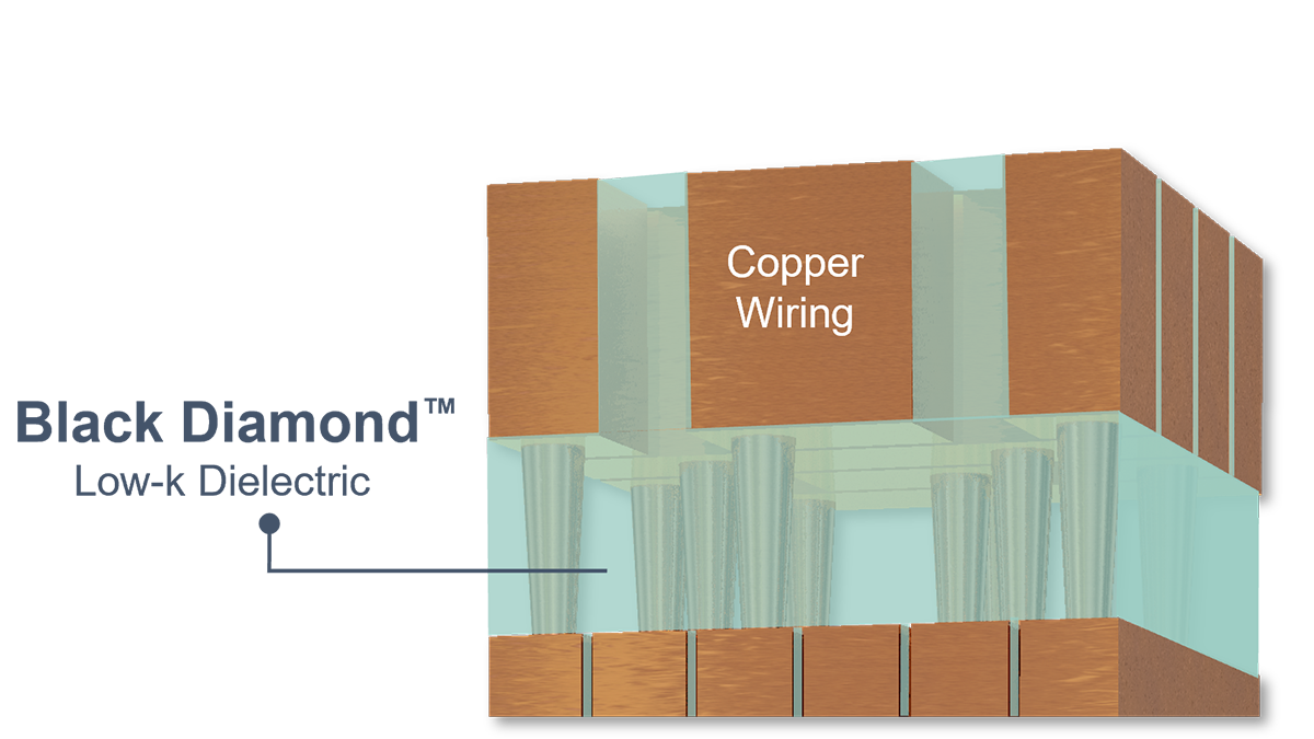
Applied Materials today introduced an enhanced version of the company’s Producer™ Black Diamond™ PECVD dielectric film. This new material enables chip scaling to 2nm and below, while offering increased mechanical strength to help take 3D logic and memory stacking to new heights.
The main DRAM and logic chip manufacturers are all implementing the most recent Black Diamond technology.
New Binary Metal Liner Enables Ultrathin Copper Wires
Chipmakers etch each layer of low-k film to facilitate chip wiring scaling. Next, they deposit a barrier layer to stop copper from migrating into the chip and causing yield problems. Subsequently, a liner is coated to the barrier to provide adhesion during the final copper reflow deposition process, which gradually fills the residual volume with copper.
The barrier and liner occupy a growing proportion of the wiring volume as chipmakers scale up their wiring, making it physically difficult to create low-resistance, void-free copper wiring in the available area.
Today, Applied Materials officially revealed its latest IMS™ (Integrated Materials Solution™) which integrates six different technologies in one high-vacuum system, including an industry-first combination of materials that enables chipmakers to scale copper wiring to the 2nm node and beyond.
The solution is a binary metal combination of ruthenium and cobalt (RuCo), which simultaneously produces better surface properties for void-free copper reflow, lowers electrical line resistance by up to 25 percent to improve chip performance, and reduces liner thickness by 33 percent to 2 nm.
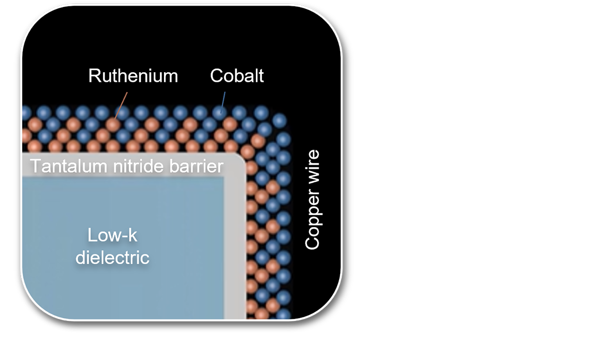
With the semiconductor industry’s first use of ruthenium in high-volume production, Applied Materials’ new binary metal combination of ruthenium and cobalt (RuCo) enables copper chip wiring to be scaled to the 2nm node and beyond and reduces electrical line resistance by as much as 25 percent.
Leading logic chipmakers have embraced the innovative Applied Endura Copper Barrier Seed IMS with Volta Ruthenium CVD*, which started shipping to customers at the 3nm node.
“An animation of the technology can be viewed here.”
Customer Comments
“While advances in patterning are driving continued device scaling, critical challenges remain in other areas including interconnect wiring resistance, capacitance and reliability,” said Sunjung Kim, VP & Head of Foundry Development Team at Samsung Electronics. “To help overcome these challenges, Samsung is adopting multiple materials engineering innovations that extend the benefits of scaling to the most advanced nodes.”
“The semiconductor industry must deliver dramatic improvements in energy-efficient performance to enable sustainable growth in AI computing,” said Dr. Y.J. Mii, Executive Vice President and Co-Chief Operating Officer at TSMC. “New materials that reduce interconnect resistance will play an important role in the semiconductor industry, alongside other innovations to improve overall system performance and power.”
A Growing Wiring Opportunity
When it comes to chip wiring process technology, Applied is a leading player of the industry. The number of interconnect wire steps has roughly tripled from the 7nm node to the 3nm node.
This means that Applied’s serviced available market opportunity in wiring has increased by more than $1 billion every 100,000 wafer starts per month (100K WSPM) of greenfield capacity, or over $6 billion. Future projections indicate that Applied’s wiring opportunity might rise to about $7 billion, or an additional $1 billion every 100K WSPM, with the implementation of backside power distribution.
The new chip wiring products, along with other materials engineering innovations for making future AI chips, will be discussed at Applied’s SEMICON West 2024 Technology Breakfast.
