


The first-ever 300 mm power gallium nitride (GaN) wafer technology has been successfully developed, according to a statement from Infineon Technologies.
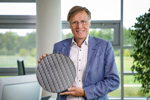
Being the first company in the world to successfully implement 300 mm power GaN technology in a scalable, current high-volume manufacturing environment will be now Infineon.
Putting Infineon at The Forefront of GaN Power Semiconductor Market
This innovation is said to significantly propel the GaN-based power semiconductor market. Since the larger wafer diameter allows for 2.3 times as many chips to be produced per wafer, chip fabrication on 300 mm wafers is both technologically more advanced and much more efficient than on 200 mm wafers.
Industrial, automotive, consumer, computing, and communication applications—such as power supply for artificial intelligence (AI) systems, solar inverters, chargers and adapters, and motor-control systems—are quickly adopting GaN-based power semiconductors.
Modern GaN manufacturing techniques enable efficiency performance, smaller size, lighter weight, and cheaper total cost, which helps end users’ applications. Furthermore, they improve device performance. Moreover, the scalability of 300 mm manufacturing guarantees improved customer supply stability.
Key Takeaways
- Infineon will shape the rapidly growing GaN market with this groundbreaking GaN 300 mm technology
- Infineon leverages existing large scale 300 mm silicon manufacturing to maximize capital efficiency in GaN production
- 300 mm GaN will help achieve cost parity with silicon over time
Growing Capacity of 300 mm GaN Wafers
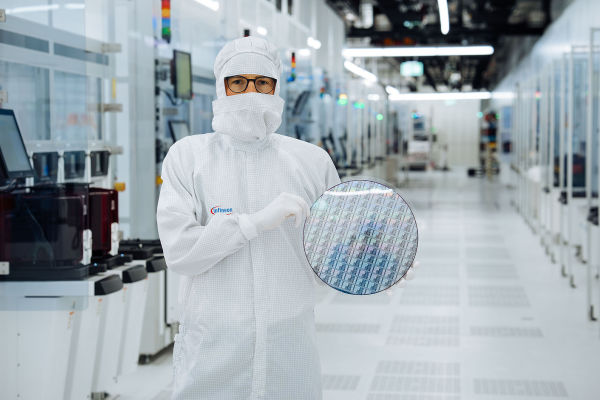
At its power fab in Villach, Austria, Infineon has successfully produced 300 mm GaN wafers on an integrated pilot line while maintaining 300 mm silicon production. The company is making use of its well-established expertise in the current 200 mm GaN and 300 mm silicon manufacture.
Infineon plans to increase GaN capacity in line with market demands. With the ability to produce 300 mm GaN, Infineon will be in a position to influence the rapidly expanding GaN market, which is predicted to reach several billion US dollars by the end of the decade.
This ground-breaking technological achievement highlights Infineon’s standing as the world leader in power systems and Internet of Things semiconductors, affirmed its official release.
With 300 mm GaN, Infineon is strengthening current solutions and opening up new application sectors. This is possible because of the technology’s more affordable value proposition and capacity to support the entire spectrum of client systems.
Because silicon and gallium nitride have relatively comparable manufacturing methods, one major benefit of 300 mm GaN technology is that it can make use of currently available 300 mm silicon manufacturing equipment.
Reliable GaN technology may be piloted on Infineon’s high-volume, 300 mm silicon production lines, which will enable faster adoption and more effective use of capital.
Cost parity for similar Si and GaN products will result from fully scaled 300 mm GaN production, which will help achieve GaN cost parity with silicon on R DS(on) level.
According to its official release, 300 mm GaN is another milestone in Infineon’s strategic innovation leadership and supports Infineon’s mission of decarbonization and digitalization.
GaN Wafer Technology at electronica Munich
The first 300 mm GaN wafer technology will be publicly displayed by Infineon during the electronica trade exhibition in Munich in November 2024.
Key Comments
“This remarkable success is the result of our innovative strength and the dedicated work of our global team to demonstrate our position as the innovation leader in GaN and power systems,” said Jochen Hanebeck, CEO of Infineon Technologies AG. “The technological breakthrough will be an industry game-changer and enable us to unlock the full potential of gallium nitride. Nearly one year after the acquisition of GaN Systems, we are demonstrating again that we are determined to be a leader in the fast-growing GaN market. As a leader in power systems, Infineon is mastering all three relevant materials: silicon, silicon carbide and gallium nitride.”