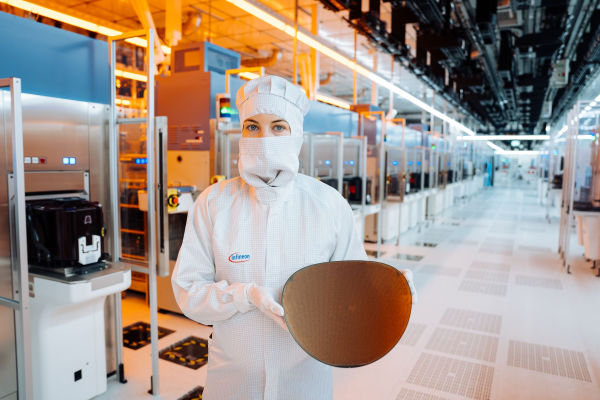
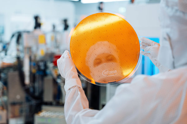
The latest milestone in semiconductor manufacturing technology was revealed by Infineon Technologies, which had previously announced the world’s first 300-millimeter gallium nitride (GaN) power wafer and opened the largest 200-millimeter silicon carbide (SiC) power fab in the world in Kulim, Malaysia.
With a thickness of only 20 micrometers and a diameter of 300 millimeters, Infineon has achieved a milestone in the handling and processing of the thinnest silicon power wafers ever produced in a large-scale semiconductor fabrication facility.
The ultra-thin silicon wafers are half as thick as the state-of-the-art wafers, which are currently 40–60 micrometers thick, and just a quarter as thick as a human hair.
Power Conversion Solutions To Get Ink A New Era
This breakthrough would greatly benefit power conversion solutions for use in AI data centers, consumer, motor control, and computer applications in terms of energy efficiency, power density, and reliability.
When compared to solutions based on traditional silicon wafers, halving a wafer’s thickness results in a 50% reduction in the substrate resistance of the wafer and a power loss reduction of over 15% in power systems.
This is especially crucial for power conversion in high-end AI server applications, because rising current levels induce rising energy demand: In this case, the CPU voltage must be lowered from 230 V to less than 1.8 V.
The vertical power supply design, which is based on vertical Trench MOSFET technology and enables a very close connection to the AI chip processor, is enhanced by ultra-thin wafer technology, which lowers power loss and improves overall efficiency.
Since the metal stack holding the chip on the wafer is thicker than 20 micrometers, Infineon engineers had to develop a novel and distinctive wafer grinding technique to get beyond the technological obstacles in lowering wafer thickness to the order of 20 micrometers.
This has a big impact on how the tiny wafer’s backside is handled and processed. Furthermore, the backside assembly procedures that guarantee the stability and superior durability of the wafers are significantly impacted by technical and production-related issues such as wafer bow and wafer separation.
20 Micrometer Thin Wafer Process
Building on Infineon’s current manufacturing experience, the 20-micrometer thin wafer process guarantees the highest yield and supply security by enabling the new technology to be seamlessly integrated into high-volume Si production lines without requiring additional manufacturing complexity.
Infineon’s Integrated Smart Power Stages (DC-DC converter) have already been supplied to the first customers, demonstrating the technology’s qualification and use. As the owner of a robust portfolio of patents pertaining to 20-micrometers wafer technology, it highlights the company’s innovation leadership in semiconductor production.
Infineon anticipates that the current standard wafer technology for low voltage power converters will be replaced in the next three to four years due to the current acceleration of ultra-thin wafer technology.
This innovation strengthens Infineon’s dominant position in the industry by offering the widest range of products and technologies, including devices based on silicon, silicon carbide, and gallium nitride—all of which are essential for decarbonization and digitization.
 Key Comments
“The world’s thinnest silicon wafer is proof of our dedication to deliver outstanding customer value by pushing the technical boundaries of power semiconductor technology,” said Jochen Hanebeck, CEO at Infineon Technologies. “Infineon’s breakthrough in ultra-thin wafer technology marks a significant step forward in energy-efficient power solutions and helps us leverage the full potential of the global trends decarbonization and digitalization. With this technological masterpiece, we are solidifying our position as the industry’s innovation leader by mastering all three relevant semiconductor materials: Si, SiC and GaN.”
“The new ultra-thin wafer technology drives our ambition to power different AI server configurations from grid to core in the most energy efficient way,” said Adam White, Division President Power & Sensor Systems at Infineon. “As energy demand for AI data centers is rising significantly, energy efficiency gains more and more importance. For Infineon, this is a fast-growing business opportunity. With mid-double-digit growth rates, we expect our AI business to reach one billion euros within the next two years.”
Putting Infineon at The Forefront of GaN Power Semiconductor Market
This innovation is said to significantly propel the GaN-based power semiconductor market. Since the larger wafer diameter allows for 2.3 times as many chips to be produced per wafer, chip fabrication on 300 mm wafers is both technologically more advanced and much more efficient than on 200 mm wafers.
Industrial, automotive, consumer, computing, and communication applications—such as power supply for artificial intelligence (AI) systems, solar inverters, chargers and adapters, and motor-control systems—are quickly adopting GaN-based power semiconductors.
Infineon will present the first ultra-thin silicon wafer publicly at electronica 2024 from 12 to 15 November in Munich (Hall C3, Stand 502).


