


The Indian GaN startup, whose name remains under wraps due to ongoing regulatory disclosures, has entered into a multi-pronged collaboration with Japanese foundries, research institutions, and materials suppliers. The focus is to leverage Japan’s mature semiconductor infrastructure and expertise in GaN epitaxy, wafer processing, and device fabrication.
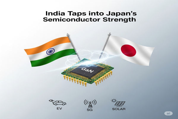
In a strategic move aimed at scaling its technological capabilities and expanding into global markets, an Indian gallium nitride (GaN) semiconductor startup has announced a key partnership with multiple players in Japan’s advanced semiconductor ecosystem.
The collaboration marks a significant milestone for India’s deep-tech semiconductor landscape, particularly in the emerging field of GaN-based devices, which are rapidly becoming central to next-generation power electronics, 5G communications, and electric mobility solutions.
Strategic Partnership for Advanced Manufacturing and R&D
The Indian startup, whose name remains under wraps due to ongoing regulatory disclosures, has entered into a multi-pronged collaboration with Japanese foundries, research institutions, and materials suppliers. The focus is to leverage Japan’s mature semiconductor infrastructure and expertise in GaN epitaxy, wafer processing, and device fabrication.
“Japan has decades of proven excellence in GaN materials, cleanroom manufacturing, and quality control. This partnership is not just about accessing their supply chain — it’s about co-creating a new generation of high-efficiency, compact power devices,”
The Indian firm will reportedly gain access to a fabrication facility in Kyushu and will co-develop GaN power transistors optimized for electric vehicle inverters and telecom base stations. Joint R&D will also be pursued with a Tokyo-based national research university to enhance device reliability and thermal management.
Mutual Benefits in a Shifting Global Supply Chain
Japan’s semiconductor sector — once the global leader — has been undergoing a revival, bolstered by renewed government investment and reshoring policies. For Indian companies seeking cutting-edge manufacturing, Japan offers stability, technical talent, and high-yield production capacity.
Experts see the partnership as a timely move amid global supply chain diversification away from China and Taiwan. “India’s GaN capabilities are still nascent, but with the right partnerships, it can leapfrog into global relevance. Japan is a natural partner due to its strengths in materials science and IP depth,” noted Dr. Sachin Mehra, a semiconductor policy expert at IIT Bombay.
On the Japanese side, the collaboration is seen as a way to tap into India’s growing domestic market for EVs, industrial automation, and renewable energy — all of which are likely to demand high-efficiency GaN components in the coming years.
India’s Growing Focus on GaN Semiconductors
The Indian government has identified compound semiconductors, including GaN and SiC, as key areas of strategic interest. Under its INR76,000 crore semiconductor incentive scheme, several startups and academic institutions are pushing GaN technology for both power and RF applications.
This new Indo-Japanese alliance could serve as a model for future collaborations in the compound semiconductor space. With global GaN device demand expected to surpass $2.5 billion by 2027, the partnership places the Indian firm in a strong position to serve both domestic and export markets.
Industry Response and Next Steps
Industry watchers view the move as a signal of growing maturity in India’s semiconductor startup ecosystem.
“This is the kind of bold cross-border alignment we need. The know-how from Japan and the entrepreneurial drive from India could produce some truly world-class innovations in GaN,”
Said Hiroshi Tanaka, a senior advisor at the Japan Semiconductor Industry Association (JSIA).
The company is expected to announce its first co-developed prototypes by late 2025, with production scaling targeted for 2026. The firm also hinted at plans to build a domestic packaging and testing unit in India to complete the supply chain loop.
As geopolitical dynamics and technology imperatives continue to reshape the global semiconductor narrative, such bilateral moves underscore how cooperation — not isolation — is the real driver of innovation.