


Researchers at the Indian Institute of Technology, Guwahati, have developed a novel machine learning (ML) framework called “LEAP.” This new technology named, LEAP is said to have led to substantial breakthroughs in the field of Electronic Design Automation (EDA).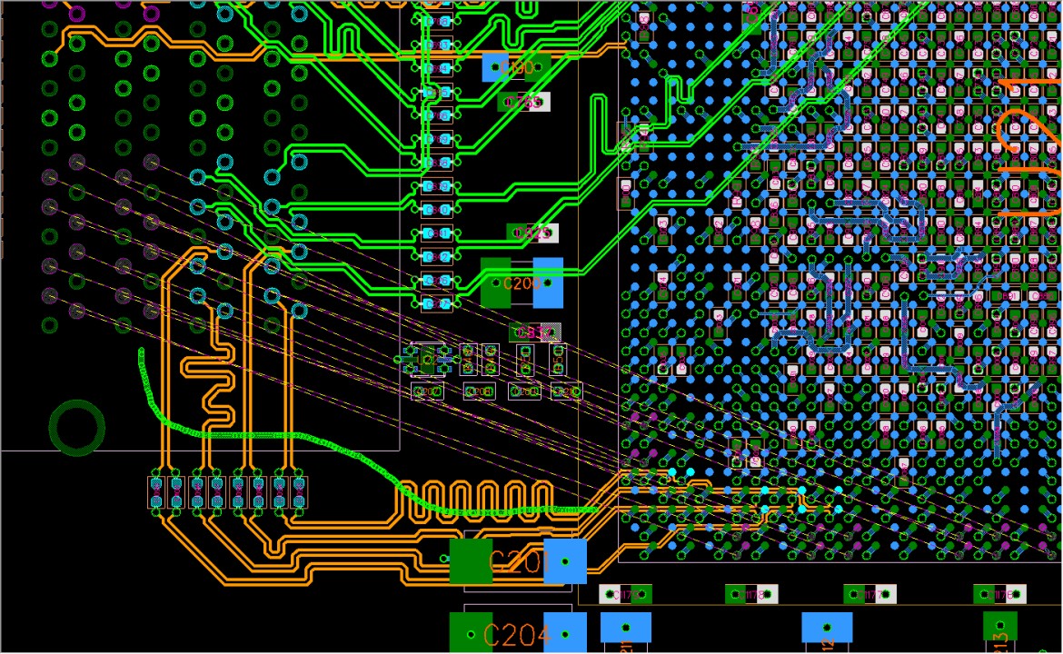
The design of Integrated Circuits (ICs), a vital part of the $600 billion semiconductor industry that fuels contemporary electronic devices, is improved by this state-of-the-art technology.
The Importance of EDA Software in IC Design
EDA software, which converts high-level designs into the Graphic Design System (GDS) production format, is essential to the manufacture of integrated circuits (ICs). However, negotiating complicated difficulties that can be difficult to overcome is a part of designing ICs.
Heuristic approaches, which are rapid problem-solving techniques that identify workable solutions without necessarily reaching perfection, are frequently used in traditional methods. Although these methods aid in balancing runtime and design quality, they frequently produce less-than-ideal outcomes.
A LEAP Breakthrough in IC Design
In response to these obstacles, the Department of Computer Science and Engineering at IIT Guwahati’s Prof. Chandan Karfa, Associate Professor, and Dr. Sukanta Bhattacharjee, Assistant Professor, along with their BTech students, Mr. Chandrabhushan Reddy Chigarapally and Mr. Harshwardhan Nitin Bhakkad, have utilized machine learning to increase the effectiveness of IC design.
Dr. Animesh Basak Chowdhury, from New York University in the United States is the other collaborator. Within EDA, their LEAP framework simplifies the technology mapping procedure. By intelligently identifying and prioritizing the most viable possibilities, LEAP reduces the amount of configurations the mapping tool needs to analyze by approximately 50%, instead of assessing thousands of possible combinations.
Speaking about the research, Prof. Chandan Karfa said, “Our framework not only speeds up the mapping process but also improves the performance of the circuits. We have reduced the runtime of the EDA tool by 50% and achieved a 2% reduction in clock period without increasing the area required for the circuits, making our solution a significant advancement in electronic design automation.”
While the old technique assesses over 250 variations, LEAP merely chooses the best 10 alternatives for each node in the design and estimates the delay for each configuration. This focused approach improves overall efficiency and simplifies the procedure.
The LEAP framework developed by IIT Guwahati showed a 50% runtime improvement and a 51% reduction in the number of configurations checked in comprehensive testing on 21 different designs. The open-source ABC EDA tool’s runtime is greatly increased by LEAP, which uses 63% less configurations to obtain comparable performance outcomes to exhaustive mapping approaches.
Impact of LEAP in the Semiconductor Sector
The semiconductor sector, which is crucial to the advancement of electrical devices like computers and cellphones, would be impacted practically by this research. Researchers can shorten design times and boost performance by optimizing the IC design process with the LEAP framework.
This results in speedier, more energy-efficient electronics that benefit customers in the long run and spur innovation in a variety of technology-related fields.
Published in the ACM/IEEE International Conference on Computer-Aided Design (ICCAD 2024) are the encouraging outcomes of this promising effort.
