


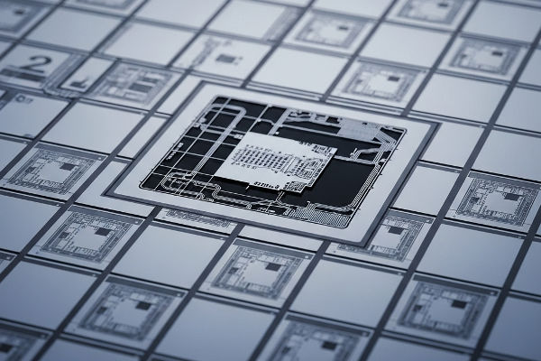
 Transistor Reinvention at the Atomic Frontier
The relentless drive to shrink transistor nodes—once defined by Moore’s Law—is encountering the atomic limit. As FinFETs, the workhorse of the last decade, reach their physical and electrical performance boundaries, the industry is embracing a successor: Gate-All-Around (GAA) transistors. Unlike its predecessors, GAA offers full gate control, redefining how electrons move in ultra-dense integrated circuits.
GAA isn’t merely a transistor evolution—it is a complete rethinking of gate architecture. Its adoption is central to the semiconductor roadmap at 3nm, 2nm, and below. This exclusive article explores the deep science, fabrication complexity, design considerations, industry adoption, and its immense implications for mobile computing, AI, HPC, and beyond.
Evolution of Transistor Architecture: From Planar to GAA
To understand the importance of GAA, we must first trace the lineage of transistor innovation:
| Generation | Technology | Node Scaling | Key Innovation | Status |
|---|---|---|---|---|
| Planar CMOS | Planar MOSFET | >65nm | Lateral gate control | Obsolete |
| FinFET (3D) | Tri-Gate FET | 22nm to 5nm | Vertical fins, partial wrap gate | Current |
| GAA (3D Nanosheet) | Gate-All-Around | ?3nm | Full gate wrap, vertical stacking | Emerging |
GAA Basics: How It Works
GAA devices are built on nanowires or nanosheets. These tiny conductive channels are surrounded on all four sides by the gate, providing improved electrostatic integrity and minimizing short-channel effects (SCE).
- Nanosheet FETs are an extension of nanowire FETs with wider, flat conducting channels for better drive current.
- Multiple nanosheets can be vertically stacked, allowing transistor design to scale in 3D for higher performance and density.
This architecture gives designers the ability to tune width, height, and number of sheets to optimize between power, area, and performance.
Why FinFETs Fall Short at 3nm and Beyond
While FinFETs revolutionized the 22nm to 5nm nodes, their architecture imposes rigid constraints on channel width and electrostatic control:
Challenges in FinFET:
- Non-uniform gate coverage (only 3 sides)
- Channel height is fixed, limiting drive current scaling
- Increased parasitic capacitance and leakage below 5nm
- Difficult fin pitch scaling for high-density designs
Advantages of GAA Over FinFET:
| Metric | FinFET | GAA (Nanosheet) |
|---|---|---|
| Gate Control | Partial (3 sides) | Full (4 sides) |
| Short Channel Control | Moderate | Excellent |
| Performance Tuning | Rigid fin width | Tunable sheet width |
| Power Consumption | Higher at low nodes | Lower |
| Stackability | No | Yes (multi-stack capable) |
In essence, GAA offers a customizable transistor geometry, vital for AI SoCs, mobile chipsets, and low-leakage server designs.
Inside GAA Transistor Design: Nanosheet Engineering
What Are Nanosheets?
Nanosheets are thin, wide silicon channels (~10–30 nm wide, ~5 nm thick) that replace the narrow fins in FinFETs. These sheets are etched from a silicon–germanium (SiGe) superlattice, with sacrificial layers removed to suspend each nanosheet.
Fabrication Flow (Simplified):
- Epitaxial growth of alternating Si/SiGe layers
- Patterning and etching to define transistor regions
- Selective SiGe removal to suspend Si nanosheets
- Gate dielectric deposition
- Metal gate wraparound deposition
- Source/Drain epitaxy and contact formation
Each of these steps requires sub-nanometer precision, EUV lithography, and multi-patterning to ensure alignment.
GAA Across the Industry: Deep Dive by Company
Samsung Foundry: Pioneers of GAA Mass Production (MBCFET)
- Technology: Multi-Bridge Channel FET (MBCFET) at 3nm
- Commercial Chips: Started shipping in late 2023
- Features:
-
-
Tunable nanosheet width
-
Improved current density
-
30% performance uplift over FinFET
-
50% power reduction

-
Samsung uses EUV + GAA, aiming to maintain leadership over TSMC in advanced nodes.
TSMC: The GAA Juggernaut at 2nm (N2 Node)
- Tech: Nanosheet GAA FET
- Timeline: Risk production in 2024, volume ramp in 2025
- Target Markets: Apple, AMD, NVIDIA, Qualcomm
- Differentiators:
-
-
High-performance drive current (IDsat > 1.6 mA/µm)
-
Designed for HPC and mobile synergy
-
Integrated backside power delivery under exploration
-
TSMC aims to integrate GAA + backside power in future A16 and N1.4 nodes.
Intel: RibbonFET and PowerVia – Dual Disruption
- RibbonFET: Intel’s GAA flavor, debuting with Intel 20A
- PowerVia: First backside power delivery in production
- Timeline: Meteor Lake ? Arrow Lake ? Lunar Lake ? Panther Lake (20A)
Intel’s GAA enables higher transistor density while PowerVia reduces IR drops and improves power efficiency—critical for AI and xPU architectures.
Design Tools and IP Migration Challenges
Migrating from FinFET to GAA requires:
- EDA Tool Upgrades: Synopsys, Cadence, and Siemens now offer nanosheet-aware layout tools
- New PDKs: Process Design Kits for nanosheet spacing, gate lengths, and sheet tuning
- IP Porting: SRAM cells, standard cell libraries, and interface IP (PCIe, DDR, USB) must be redesigned for GAA pitch and timing
Design for manufacturability (DFM) also becomes critical to avoid yield loss from alignment errors or gate oxide variation.
Market Impact: From Edge AI to Data Centers
Mobile Devices
GAA SoCs will dominate flagship smartphones starting in 2025-26, driven by Apple (TSMC N2) and Samsung Exynos (MBCFET).
High-Performance Computing
Datacenter chips—like AMD Instinct and NVIDIA Blackwell—will benefit from GAA’s thermal and electrical efficiency.
Automotive
As EV chips move to 5nm and beyond, GAA offers better high-temperature stability and voltage reliability.
Edge AI & IoT
Small form-factor edge AI chips (from companies like SiFive, Esperanto) will benefit from nanosheet-driven power savings.
GAA Manufacturing Bottlenecks and Risks
1. Yield Challenges
Stacked nanosheets can cause defects at interface layers, leading to variability and poor performance.
2. Process Variability
Thin sheet fabrication demands atomic-scale control. Small deviations in etch depth or gate metal deposition can cause massive variability in current flow.
3. Cost Escalation
GAA nodes, combined with EUV and advanced metrology tools, are 30–50% costlier per wafer than 5nm FinFETs.
4. Reliability and Reliability Models
Hot-carrier injection (HCI), bias temperature instability (BTI), and time-dependent dielectric breakdown (TDDB) are still being characterized for nanosheet materials.
Future of GAA and Beyond
3D GAA + CFET
Complementary FETs (CFETs) stack NMOS over PMOS vertically, doubling density. GAA is a prerequisite for CFET.
New Materials
- Germanium (Ge) or III-V materials for channel mobility
- High-k dielectrics for better gate control
- 2D materials like MoS? for ultra-thin nanosheets
Fully 3D Integrated Systems
In the future, GAA may be fused with 3D chiplet integration and optical interconnects for near-zero latency designs.
GAA as the Next Great Leap
Gate-All-Around transistors represent more than a scaling breakthrough—they symbolize the continued vitality of the semiconductor roadmap.
As compute demands accelerate—driven by AI, mobile, automotive, and edge workloads—GAA provides the efficiency, customizability, and performance essential for the next decade of innovation.
With Intel, Samsung, and TSMC advancing on parallel paths, the era of GAA will define leadership in logic manufacturing through the late 2020s and early 2030s. This is not just a new transistor—it is the future substrate of intelligence itself.