


Providing new insights into semiconductor doping and improving the performance of GaN devices
According to a study conducted by Nagoya University in Japan, a unique superlattice structure is formed by the straightforward thermal reaction of gallium nitride (GaN) with metallic magnesium (Mg). This is the first time that the introduction of 2D metal layers into a bulk semiconductor has been recognized by researchers. The materials were closely observed using a variety of state-of-the-art characterisation techniques, and this allowed the researchers to gain new insights into the semiconductor doping and elastic strain engineering processes.
An essential wide bandgap semiconductor material called GaN is about to take the place of conventional silicon semiconductors in applications that require quicker operating frequencies and larger power densities. Gan-based devices are getting viability in many applications, such as gadgets like LEDs, laser diodes, and power electronics, including vital parts of electric cars and rapid chargers. These unique properties of GaN confer its value.
P-type and n-type electrical conductivity are the two fundamental and complimentary forms found in semiconductors. Whereas the n-type semiconductor conducts electricity through free electrons, the p-type semiconductor is predominantly composed of free carriers carrying positive charges, or holes. Doping is the deliberate injection of certain impurities (dopants) into a pure semiconductor material to modify its electrical and optical characteristics, giving a semiconductor p-type or n-type conductivity.
To yet, only Mg has been found to provide p-type conductivity in the field of GaN semiconductors. The whole process, including the solubility limit and segregation behavior of Mg, are still unknown despite the fact that doping Mg into GaN has been successfully accomplished for 35 years. Their optimization for optoelectronics and electronics is limited by this uncertainty.
How To Improve The Conductivity of p-type GaN
Jia Wang, the study’s primary author, and his associates carried out an experiment in which they systematically placed metallic Mg thin films on GaN wafers and heated them to a high temperature, a process known as annealing, in order to increase the conductivity of p-type GaN.
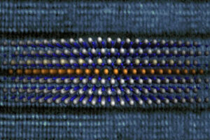
The scientists saw the spontaneous development of a superlattice with alternating layers of GaN and Mg using cutting-edge electron microscope imaging. This is particularly strange because the physical characteristics of Mg and GaN are very different from one another.
“Although GaN is a wide-bandgap semiconductor with mixed ionic and covalent bonding, and Mg is a metal featuring metallic bonding, these two dissimilar materials have the same crystal structure, and it is a strikingly natural coincidence that the lattice difference between hexagonal GaN and hexagonal Mg is negligibly small,” Wang said. “We think that the perfect lattice match between GaN and Mg greatly reduces the energy needed to create the structure, playing a critical role in the spontaneous formation of such a superlattice.”
The researchers discovered that the host material experiences compressive strain as a result of this unusual intercalation activity, which they dubbed interstitial intercalation. It was discovered that the Mg layers being put into the GaN endure a tension of more than 20 GPa, which is the largest compressive strain ever recorded in a thin-film material.
This stress is comparable to 200,000 times atmospheric pressure. This is far higher than the typical silicon film compressive stresses, which are in the range of 0.1 to 2 GPa. This strain can lead to major changes in the electrical and magnetic characteristics of electronic thin films. The electrical conductivity of GaN via hole transport was considerably increased along the stressed direction, the researchers discovered.
“Using such a simple and low-cost approach, we were able to enhance the transport of holes in GaN, which conducts more current,” Wang said. “This interesting finding in interactions between a semiconductor and a metal may provide new insights into semiconductor doping and improve the performance of GaN-based devices.”