


Fujifilm Corporation has inaugurated a state-of-the-art development and evaluation facility at its Shizuoka Factory in Japan, marking a major step to enhance its semiconductor materials operations amid booming demand from AI, 5G, and IoT sectors.
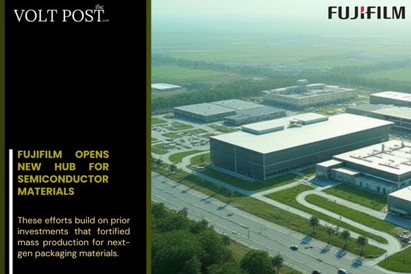
To fast-track innovations in semiconductor materials amid surging global demand, spanning 6,400 square meters, the new building features ultra-clean cleanrooms equipped with cutting-edge testing equipment for rigorous performance assessments of prototype materials.
Advanced AI-powered image recognition technology now identifies minute contaminants, elevating quality control precision for products including EUV resists, ArF immersion materials, PFAS-free alternatives, nanoimprint lithography compounds, and the innovative WAVE CONTROL MOSAIC technology for image sensors.
A dedicated digital transformation team integrates AI into manufacturing workflows, enabling scalable production with minimal defects and supporting everything from legacy nodes to cutting-edge processes.?
Ramping Up Polyimide Production For Advanced Chip Packaging
Fujifilm’s semiconductor materials division saw sales grow about 1.7 times between fiscal years 2021 and 2024, establishing it as a key growth engine for the group, with over 100 billion yen invested in facilities during that period.
The company plans another 100 billion yen or more from fiscal 2025-2026 to ramp up polyimide production for advanced chip packaging and meet surging needs for AI semiconductors.
This hub accelerates one-stop solutions covering photoresists, CMP slurries, cleaners, thin-film chemicals, and high-purity process aids across front-end and back-end fabrication.?
 Market Outlook
The global advanced semiconductor sector is projected to double by 2030, driven by AI data centers and connected devices, positioning the company to capture more share through global manufacturing in Japan, the US, Europe, and Asia.
Complementary moves include planned semiconductor materials plants in India for regional exports and expanded capacity in Taiwan, underscoring a robust supply chain strategy.
These efforts build on prior investments that fortified mass production for next-gen packaging materials.?
Key Comments
“This new facility strengthens our ability to evaluate development products swiftly, speeding up innovations in advanced semiconductors while ensuring stable, high-quality supplies,” Fujifilm stated, emphasizing AI-driven defect detection and DX for process optimization. Executives highlighted the role in leading market growth: “Fujifilm will expand its semiconductor materials business to support the advanced information society, leveraging broad portfolios from wafer processing to packaging.” They reaffirmed commitment to diverse customer demands via resilient global bases.