


The new system extends ASM’s portfolio of industry benchmark single-wafer silicon carbide epitaxy systems, the 6” PE1O6 and 8” PE1O8 systems, with a higher throughput, lower cost of ownership, dual chamber, single wafer, 6” and 8” compatible, silicon carbide epitaxy system.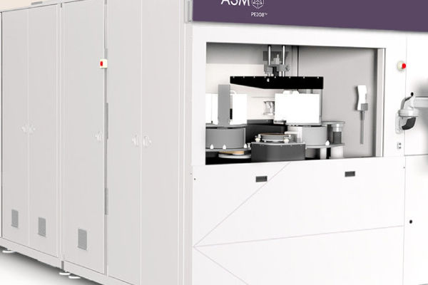
ASM International presented the PE2O8 silicon carbide epitaxy system at the 2024 International Conference on Silicon Carbide and Related Materials.
The company claims it to be a revolutionary dual-chamber platform for silicon carbide (SiC) epitaxy (Epi).
The PE2O8 is the benchmark epitaxy system for low defectivity, high process uniformity, increased throughput, and low cost of ownership—all of which are necessary to enable widespread adoption of SiC devices. It was designed to meet the demands of the advanced SiC power devices market.
The general trend toward electrification is pushing more power device makers to use SiC for an increasing number of high-power applications (like advanced data centers, green power, and electric vehicles).
As a result of this increased demand and the need for SiC to be more affordable, 6″ to 8″ SiC substrates are becoming more and more popular. Simultaneously, producers of SiC devices are developing more powerful devices that will gain from improved SiC epitaxy.
Utilizing a unique architecture, the dual chamber PE2O8 system deposits SiC with ultra precise control, enabling significantly greater yield and higher throughput. Both great productivity and low operating expenses are made possible by the extremely compact, dual chamber design.
The system also has an easy preventative maintenance strategy that lowers the incidence of unscheduled downtime and increases uptime. Deliveries of the system have been continuing to a number of clients worldwide, including manufacturers of SiC power devices.
With a better throughput and a low cost of ownership, the new system expands ASM’s line of industry-standard single wafer silicon carbide epitaxy systems, which are the 6″ PE1O6 and 8″ PE1O8 systems. It is a dual chamber, single wafer, compatible with both 6″ and 8″ silicon carbide epitaxy systems.
Since 2022, ASM has been developing and perfecting its single wafer SiC epitaxy technology through its new SiC Epi product unit. The market for SiC epitaxy equipment has expanded significantly in recent years due to the structurally increased demand for electric vehicles and improvements in SiC wafer and device yield overall.
Key Comments
“We are at a critical inflection for silicon carbide power products, as our customers transition from 6” to 8” wafers”, said Steven Reiter, Corporate Vice President, and business unit head of Plasma and Epi at ASM. “Delivering a high-quality epitaxy process on larger wafers with defectivity control is critical, and we have been the industry benchmark for process uniformity with our novel chamber design. We have now extended our system capability to improve our process control and our value for customers with lower cost of ownership.”
For Further Info: CLICK HERE