


Introduction to 2.5D and 3D Hybrid Bonding Packaging
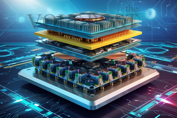
As semiconductor technology continues to evolve, the need for advanced packaging solutions has become more pressing. Two of the most significant advancements in this field are 2.5D and 3D hybrid bonding packaging, which offer improved performance, power efficiency, and miniaturization compared to traditional methods.
These techniques are crucial for high-performance computing (HPC), artificial intelligence (AI), data centers, and mobile devices. This article explores the fundamentals of 2.5D and 3D hybrid bonding, their advantages, challenges, applications, and future trends.
Understanding 2.5D and 3D Hybrid Bonding
What is 2.5D Packaging?
2.5D packaging is an intermediate approach between traditional 2D and full 3D stacking. It involves mounting multiple integrated circuits (ICs) on a silicon interposer, which enables better connectivity and thermal management. The interposer provides a platform for different chips to communicate efficiently with reduced signal loss.
What is 3D Packaging?
3D packaging, on the other hand, takes integration a step further by stacking dies directly on top of each other using through-silicon vias (TSVs) or hybrid bonding. This method offers reduced footprint, lower power consumption, and faster data transfer speeds, making it ideal for applications demanding high performance and compact designs.
Hybrid Bonding: The Game-Changer
Hybrid bonding is a breakthrough technique that allows direct bonding of wafers or dies at a molecular level without requiring solder bumps. This enables ultra-dense interconnects, significantly reducing interconnect resistance and enhancing performance. Hybrid bonding is a key enabler for both 2.5D and 3D packaging strategies.
Advantages of 2.5D and 3D Hybrid Bonding Packaging
- Higher Bandwidth and Performance – Shorter interconnect paths enable faster signal transmission and higher data rates.
- Lower Power Consumption – Efficient interconnects lead to reduced power leakage and lower operating power.
- Smaller Form Factor – Eliminates the need for large PCBs and external interconnects, making devices more compact.
- Improved Thermal Management – Advanced cooling solutions and better heat dissipation techniques enhance reliability.
- Enhanced Heterogeneous Integration – Allows different types of chips (logic, memory, RF, etc.) to be integrated into a single package.
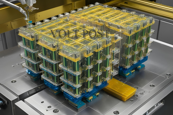
Technical Aspects of Hybrid Bonding
Bonding Process
- Surface Preparation – Ensuring atomically clean and smooth surfaces to enable direct contact.
- Alignment and Contact – High-precision alignment of dies or wafers before bonding.
- Annealing – A controlled thermal process to strengthen the bond and ensure reliability.
Key Technologies Used
- Through-Silicon Vias (TSVs) – Essential for vertical connections in 3D packaging.
- Die-to-Wafer (D2W) and Wafer-to-Wafer (W2W) Bonding – Different approaches depending on integration needs.
- Copper-to-Copper Hybrid Bonding – Eliminates the need for solder bumps, reducing resistance and improving signal integrity.
Challenges & Solutions
1. Alignment Accuracy
Challenge: Maintaining sub-micron alignment precision.
Solution: Advanced lithography and metrology techniques.
2. Thermal Management
Challenge: Heat dissipation in stacked structures.
Solution: Innovative cooling solutions, including liquid cooling and thermal vias.
3. Manufacturing Yield
Challenge: Defect rates in bonding can affect overall yield.
Solution: Improved wafer inspection and adaptive bonding techniques.
4. Cost Considerations
- Challenge: Higher initial costs due to complex processes.
- Solution: Economies of scale and process optimizations to reduce manufacturing expenses.
Applications of 2.5D and 3D Hybrid Bonding Packaging
- Artificial Intelligence (AI) and Machine Learning – High bandwidth and low latency are critical for AI accelerators.
- High-Performance Computing (HPC) – Used in data centers, supercomputers, and cloud computing applications.
- Mobile Devices – Enhances smartphone processors, memory integration, and power efficiency.
- Automotive Electronics – Key for advanced driver-assistance systems (ADAS) and autonomous vehicles.
- Internet of Things (IoT) – Compact and energy-efficient designs are ideal for smart devices and edge computing.
Future Trends and Innovations
1. Advanced Materials
- The use of novel materials such as graphene and nanowires can further improve interconnect efficiency.
2. Monolithic 3D Integration
- Directly integrating multiple layers of transistors on a single die for even higher performance and density.
3. AI-Driven Packaging Optimization
- Machine learning techniques to optimize chiplet placement and bonding processes.
4. Integration with Photonics
- Optical interconnects for ultra-high-speed data transmission.
2.5D and 3D hybrid bonding packaging represent the future of semiconductor integration, offering unmatched performance, efficiency, and miniaturization.
While challenges exist, ongoing advancements in materials, manufacturing, and cooling techniques are paving the way for broader adoption. As demand for high-speed, energy-efficient devices grows, these advanced packaging methods will play a crucial role in shaping the future of technology.
Here are some key references for 2.5D and 3D hybrid bonding packaging:
- Intel’s Advanced Packaging (Foveros & EMIB) – Intel Packaging
- TSMC 3DFabric & CoWoS Technologies – TSMC 3DFabric
- IEEE Paper on Hybrid Bonding – IEEE Xplore
- UCIe Standard for Chiplet Integration – IEEE UCIe
