


Intel Leads Semiconductor Innovation with High-NA EUV Lithography. Intel High-NA EUV Lithography Achieves Major Milestone with 30,000 Wafers Processed.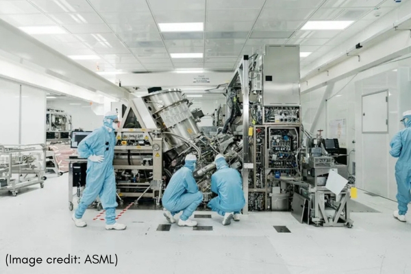
Intel High-NA EUV lithography has reached a groundbreaking milestone by successfully processing 30,000 wafers, marking a significant leap in semiconductor manufacturing. This achievement cements Intel’s position as an industry leader in next-generation chip production, paving the way for higher transistor densities and more efficient chip fabrication.
The milestone was announced at the SPIE Advanced Lithography + Patterning Conference, where Intel engineers revealed that the company had been rigorously testing ASML’s High-NA Twinscan EXE:5000 EUV lithography tools.
These advanced machines, valued at approximately €350 million each, were installed at Intel’s D1 development fab in Hillsboro, Oregon, and have now demonstrated their capability in high-precision chipmaking processes.
What is High-NA EUV Lithography?
A Game-Changer for Next-Gen Chip Production
High-NA (Numerical Aperture) Extreme Ultraviolet (EUV) lithography is an advanced chip fabrication technology designed to create smaller, more powerful semiconductors. With higher resolution patterning, High-NA EUV enables manufacturers to etch ultra-fine features onto silicon wafers, making it a critical component in achieving transistor scaling beyond Intel’s 14A (1.4nm-class) process node.
According to ASML, the leading supplier of EUV tools, High-NA technology increases lithography precision by 70% compared to standard EUV. This allows for the production of denser, more energy-efficient chips, essential for the growing demands of AI, data centers, and next-generation computing.
Intel’s Milestone: Processing 30,000 Wafers
A Testament to Advanced Chip Manufacturing
Since integrating ASML’s High-NA Twinscan EXE:5000 tools into its fab, Intel has successfully processed 30,000 wafers, demonstrating the efficiency and reliability of the new lithography system. This achievement is a significant step in Intel’s strategy to regain process leadership by 2025, particularly as it prepares for mass production using High-NA EUV technology.
Leadership Perspective: Intel’s Commitment to Innovation
Steve Carson, Senior Lithography Engineer at Intel, commented on the milestone:
“Processing 30,000 wafers with High-NA EUV tools is a testament to our dedication to pioneering semiconductor manufacturing. This milestone not only showcases the capabilities of our equipment but also sets the stage for future technological advancements.”
Dr. Martin Keller, Semiconductor Analyst at TechInsights, stated:
“Intel’s ability to process 30,000 wafers using High-NA EUV is a significant milestone in chipmaking history. This demonstrates that the technology is production-ready and scalable for future process nodes.”
Impact on the Semiconductor Industry
Accelerating the Future of Chip Manufacturing
The success of Intel High-NA EUV lithography marks a major breakthrough for the semiconductor industry. By proving that the Twinscan EXE:5000 tools can handle high-volume wafer processing, Intel paves the way for faster, more efficient chip production.
Some key benefits of High-NA EUV technology include:
- Higher resolution lithography for more powerful, efficient chips.
- Reduced production costs by enabling single-exposure patterning, eliminating the need for complex multi-patterning techniques.
- Faster manufacturing cycles, accelerating time-to-market for advanced semiconductor products.
Collaboration with ASML and Industry Leaders
Intel’s milestone also highlights its close collaboration with ASML to refine High-NA EUV technology. ASML’s roadmap suggests that the next-generation Twinscan EXE:5200 tools, expected by 2025, will further improve wafer throughput and efficiency, keeping Intel ahead of its competitors.
What’s Next for Intel?
Scaling Production for Future Chip Nodes
With the successful processing of 30,000 wafers, Intel is now focused on integrating High-NA EUV into its mass production strategy. The company aims to utilize this technology for its Intel 18A and beyond nodes, ensuring it remains at the forefront of semiconductor innovation.
Ann Kelleher, EVP and GM of Intel’s Technology Development, emphasized:
“This milestone represents a major step forward in our journey to reclaim process leadership. High-NA EUV is a critical enabler for our future roadmap, and we are committed to scaling this technology for high-volume manufacturing.”
Intel’s Vision for the Future of Semiconductor Manufacturing
The achievement of processing 30,000 wafers with High-NA EUV lithography is a landmark moment for Intel and the semiconductor industry. With next-generation chip production now within reach, Intel is poised to lead the AI-driven, high-performance computing revolution.
This breakthrough not only reinforces Intel’s technological leadership but also sets the stage for more efficient, scalable, and cost-effective semiconductor manufacturing in the years ahead.
