


According to the latest announcement from Nanusens, the company has developed an innovative approach to the problem of improving RF front ends for 6G by utilizing their groundbreaking MEMS-within-CMOS technology.
Josep Montanyà, Nanusens’ CEO, explained, “This builds on and extends the company’s work of using its unique technology to enable the upper 5G bands to be used cost effectively. We have test chips for this with customers and they are impressed with their performance and actually advised us to use this technology to also create solutions for 6G as the industry really has a challenge.
“The issue is that 6G needs to be able to handle many more and possibly higher frequencies than 5G. To do this requires additional antennas to be integrated into the phone to handle more bands but, due to them having to be smaller to fit more of them inside the phone, their efficiency decreases. In order to get the best possible performance from each antenna, each needs to be tuned to reconfigure to different bands and to avoid mismatch with the power amplifier. This is currently done by means of tunable capacitors, said Josep.”
With its patented and silicon-proven method of constructing MEMS structures using standard CMOS technologies, Nanusens has been able to simultaneously produce the control circuitry and a large number of digitally tunable nanoscale capacitors inside the CMOS layers of a chip.
Compared to competing alternatives, this integrated single chip solution is smaller and offers far superior performance because of its significantly improved linearity, which results in almost negligible distortion. Additionally, talk times are up to 30% better because to the nano-capacitors’ higher power efficiency, which resolves the existing problem of decreased efficiency.
Additionally, the problem of present antenna solutions becoming more and more power-hungry in the higher frequency bands is resolved by these RF Digitally Tunable Capacitors (DTCs). The secret is the extremely high Q factor, which is above 100 at 1GHz. More crucially, the Q factor stays high to maintain very low power losses in the upper bands, when competitors’ Q factors start to decline sharply. Practically speaking, this means that range has increased by at least 14%, which enhances user experience by reducing lost calls and bad reception regions.
Dr Marc Llamas, Nanusens’ CTO, said, “Our unique solution for the 5G and 6G RF Front End is exciting the major RF corporations that we have shown it to who need a better solution. We believe that this is RF Front End solution that they have been looking for to enable the 6G market to really take off. Not only for phones but also for other applications in industry and automotive due to its much lower latencies and data rates that are 50 times better than 5G at 1000 gigabits per second.
“That is a huge potential 6G market that is measured in the hundreds of millions of new devices a year. driven by the rapidly growing needs of data intensive applications such as AI, virtual reality, augmented reality and IoT. Our unique technology of just using standard CMOS techniques in any CMOS fab means that we can produce in virtually unlimited volumes to meet this demand, added Dr Marc.”
The issues with rival solutions of solid-state switches and RF MEMS
The issue with solid-state switches is their low Q factor. Q factors are a performance metric; higher Q factors are desirable since they signify less operational losses. The ON state (Ron) resistance of solid-state switching systems is the cause of their poor Q factor. Effective use of these higher bands is now hampered by this, which gets worse as the frequency rises to the higher 5G bands.
Due to the usage of dielectric, RF MEMS tunable capacitors have low dependability. This can experience dielectric charging, which is the primary reason why RF MEMS devices malfunction. It can also have a limit on the maximum voltage that it can sustain from peak to peak before dielectric breakdown.
Nanusens has developed a solution for both issues. It makes use of an array of RF capacitive switches and makes antenna adjustment for the higher 6G bands possible. Because there is no ON state resistance in this design, the low Q factor issue is resolved. At 1GHz, the Q factor is above 100, and crucially, it stays high to maintain very low losses in the higher bands, where competitors’ Q factors sharply decline.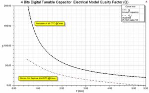
Key performance parameters
- The Q factor and linearity are important components of DTCs. At 1GHz, the Q factor exceeds 100, matching cutting-edge RF MEMS technologies and far surpassing solid-state switching solutions. Additionally, they exhibit outstanding linearity which is more than the 5G requirement of 90 dBc for IMD3.
- It is possible to maintain very minimum small capacitance, down to Coff of 30 fF for a single capacitor off state (that means a Cmin of 0.45 pF for a 4-bit DTC) and much lower for subsequent iterations.
- Similarly, Nanusens anticipates increasing the capacitance ratio from its present value of 2.2 to 4 with the next product iteration.
Solves increasing problem of parasitics
As device performance approaches ideal performance (very low, off-state capacitance (Coff) and very high Q) and new, allocated frequency bands start to move to the microwave domain, parasitics interconnects will increasingly have a negative impact on performance.
Being built using a standard CMOS means that the DTC can be made at the same time and on the same chip as other RF front end components, such as PA, LNA and transceivers, to dramatically reduce interconnect parasitics while making them reconfigurable. These single chip reconfigurable solutions will fit in ultra-small, low profile, low cost WLCSP packages and this integration also reduces the BOM and saves board area compared to competitors’ multi-component solutions.
Standard CMOS
Nanusens devices are produced in a standard CMOS fab, which allows them to take advantage of the economies of scale associated with CMOS technology. This helps them to compete with other products that are produced using more costly silicon-on-insulator/silicon-on-sapphire processes or specialized MEMS fabs.
Nanusens also benefits from the possibility to use any CMOS fab, nearly infinite manufacturing quantities, and high yields of CMOS fabs for this product. These are the normal times for producing CMOS goods, as opposed to certain competitors that require far longer times due to their non-standard nature.
How the Nanusens Use standard CMOS processes
Vapour HF (vHF) is used to etch away the Inter Metal Dielectric (IMD) through the pad openings in the passivation layer, resulting in the creation of nanostructures. After that, the holes are plugged and the chip is packed as necessary. Due to the fact that the devices may be immediately combined with active circuitry when needed and have high yields comparable to CMOS devices, they simply require typical CMOS procedures with minimum post-processing. It also implies that the output is not dependent on the fab.
For Further Info: CLICK HERE
